INTRINSIC ATOMIC DEFECTS OF LEAD CHALCOGENIDES
12.03.2024 16:43
[3. Технические науки]
Автор: Tetiana Mazur, Ph.D., Associate Professor, Ivano-Frankivsk National Technical University of Oil and Gas, Ivano-Frankivsk; Galyna Mateik, Ph.D., Associate Professor, Ivano-Frankivsk National Technical University of Oil and Gas, Ivano-Frankivsk
Lead compounds with chalcogens belong to the group of semiconductor materials of non-stoichiometric composition [1]. Although the region of stable homogeneous phase in these compounds is narrow with respect to deviation from stoichiometry in atomic percentages, it corresponds to a significant range of free charge carrier concentrations [2]. It is important to note that lead compounds have n-type conductivity when there is an excess of lead compared to the stoichiometric composition, while p-type conductivity occurs when there is an excess of chalcogens [1,2]. Thus, in the case of PbS, the hole concentration reaches 6.9 1018 cm-3 at 1123 – 1173 K, and the electron concentration reaches a maximum value of 1.6 1019 cm-3 at 1348 K with an excess of lead. For lead selenide, the maximum concentration of holes at 1073 K was 2 1019 cm-3, and the maximum concentration of 2.3 1019 cm-3 electrons was observed at 1223 K. In lead telluride, these values are as follows: 5 1018 cm-3 holes at 1053 K; 1.5 1019 cm-3 electrons at 993 K.
Today, there is a generally accepted explanation for the electrical activity of intrinsic defects in PbX compounds (where X is S, Se, Te), based on numerous calculations of the energy spectrum of vacancies of the metal VPb and chalcogen VX. According to this explanation, vacancies are doubly charged donors (VХ2+) or acceptors (VPb2+). These results are confirmed by both cluster and analytical calculations in the approximation of a centrally symmetric environment of defects. However, there are other studies indicating that crystal annealing and equilibrium diagrams can only be explained by singly charged vacancies (VPb-) and interstitial lead atoms (Pbі+). In the case of films, the defect state is explained by both singly charged Pbі+ and doubly charged chalcogen vacancies (VХ2-). Most studies consider the interstitial chalcogen atom to be electrically neutral Xі0. Regarding antistructural defects, lead in place of chalcogens is considered a doubly charged acceptor, and chalcogens S, Se, Te in place of Pb are considered doubly charged donors. To resolve this ambiguous situation regarding the electrical activity of atomic defects in lead chalcogenides, the use of calculations within the Hartree-Fock approximation was proposed. It is shown that the positions of the energy levels of lead chalcogenide vacancies are determined by electron-electron interaction and the existence of charge exchange levels of vacancies near the allowed bands is assumed.
Consequently, after analyzing various sources, we can conclude that the defect subsystem of lead chalcogenide crystals is quite complex and is probably characterized by the presence of the entire spectrum of defects. The work proposed a crystal chemical model of atomic defects in lead chalcogenide crystals, which provides for the simultaneous existence of both singly and doubly charged interstitial lead atoms (Pbі+, Pbі2+) and lead vacancies (VPb-, VPb2-).
It was found that for lead chalcogenides it is possible to change the stoichiometric composition by controlling the partial pressure of the constituent components (lead, chalcogens) above the solid phase or using a two-temperature annealing method. In this case, the equilibrium between the crystal and the vapor can be described using a system of equations of quasi-chemical reactions, which makes it possible to determine the concentrations for the entire spectrum of the defect subsystem of the crystal:
Where PPb and PX2 are the partial pressures of lead and chalcogen vapors, respectively, “V” is vapor; K = K0 exp(−ΔH/kT) – equilibrium constants (K0 and ΔH are values depending on temperature).
The proposed crystal chemical model can be used for numerical calculations of the equilibrium concentrations of current carriers and concentrations of atomic defects in all lead chalcogenides, provided that overall electrical neutrality is ensured. This is possible provided that we have sufficiently accurate values of the main equilibrium constants of quasi-chemical reactions and their temperature dependences.
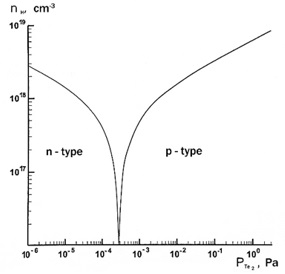
In Fig. 1 shows an example of the results of detailed calculations for the case of PbTe.
Fig. 1. Dependence of the calculated values of the Hall (nH = n-p) carrier concentration for PbTe on the telurium pressure at an annealing temperature of 833° K.
Consequently, the specified crystal chemical model makes it possible to successfully analyze the complex spectrum of defects in lead chalcogenides, depending on the technological aspects of growing crystals and thin films.
References
1. D.M. Freik, V.V. Prokopov, M.A. Galushchak, M.V. Pitz, G.D. Mateik. Crystal chemistry and thermodynamics of defects in AIV-VI compounds. Play. Ivano-Frankivsk, (2000).
2. T. Mazur, M. Mazur, G. Mateik, Study of charge carriers scattering in the two-layer n-PbTe/n-PbS heterostructure, Molecular Crystals and Liquid Crystals, (2024); https://doi.org/10.1080/15421406.2024.2310423
3. T.M. Mazur, M.P. Mazur, Study of carrier mobility in CdTe and PbTe thin films as a function of temperature, Molecular Crystals and Liquid Crystals, , 768(2), 83–88 (2024); https://doi.org/10.1080/15421406.2023.2241781

